Embedded system design [specific development procedure know-how]

Table of contents
What is Design?

This section describes the steps to be followed in the design and development process. This is intended to be somewhat informative for beginners, as each individual should follow his or her own style.
When you have an idea for a product, if you just keep it in your mind, it will remain a "pie in the sky". In order to make the concept concrete, a process called design is necessary. Designing is a process that requires specialized knowledge and skills, but in other words, it is the logical process of determining what parts to use and how to use them in order to make the idea concrete.
Of course, specialized knowledge and experience are required depending on the design, but in the design of embedded technology, it is possible with basic knowledge of electricity and electronics and some experience. This is explained in the "Basics of Embedded Technology" section, so please make sure you have a good understanding of this.
Comparing the case where a person with only programming experience handles a microcomputer and starts designing, and the case where a person with no programming experience but with some basic knowledge of electrical and electronic engineering handles a microcomputer and starts designing, the one with a basic knowledge of electrical and electronic engineering has an overwhelming advantage in acquiring embedded technology.
In design, we deal with hardware, and this is unavoidable. However, the basic knowledge of electricity and electronics required for embedded system design is not difficult, and you will be able to start designing if you have enough knowledge to understand the specifications of each component.
For example, in designing the input/output interface of a microcontroller, a component called a optocoupler is used to electrically isolate the microcontroller from the outside world.
System Design Procedures
Please refer to the following example of a system design procedure.
- Specifically state the purpose of the development
- Organize functions according to purpose (number of required in/out pins, peripherals)
- MCU selection (memory ROM/RAM, peripherals used, number of pins)
- IO map creation (assign main and alternate functions with reference to the pin map in the specification)
The above steps are the first steps in the actual design process from the conception stage of the development target. The following is an individual explanation of each step.
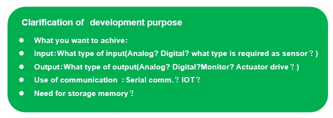
① Clearly state the purpose of the development:
Let's first summarize the objectives to concretize the development concept. In particular, since there are always inputs and outputs in a system, let's list them concretely.
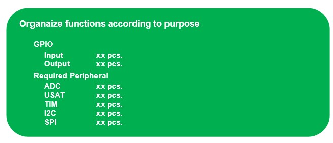
② Organize functions according to purpose:
Once the number of input/output points to be used has been determined to some extent, the specific input/output specifications are organized and classified.
First, GPIOs and peripheral functions (peripherals) are categorized. Next, determine the detailed specifications for each.
③ MCU Selection:
Once the number of input/output points and peripheral functions (peripherals) to be used are determined, MCU can be selected by specifying other flash memory ROM and RAM capacities to store the program.
Larger flash memory ROM and RAM sizes are more spacious than smaller ones, and even if RTOS is introduced, memory limitation problems are unlikely to occur. However, when introducing RTOS into actual products, it is desirable to avoid adopting unnecessarily large memory sizes in order to keep costs as low as possible.
Use a larger memory size during the learning phase to actually experience the memory (ROM and RAM) consumption according to the program and reflect this when developing the actual product.
For the Cortex-M3 core F10x series of STM32 MCUs, selection is based on system clock frequency, peripheral functions (peripherals) to be used, and number of pins. When using multiple peripherals, function allocation is easier with a type that has a larger number of pins.
For standard applications, the Cortex-M3 core F10x series is sufficient, but for applications requiring floating-point operations, select MCU with a Cortex-M4 core or higher. However, even a Cortex-M3 core can function with software emulation operations, so it is sufficient for small applications.
④ IO map creation
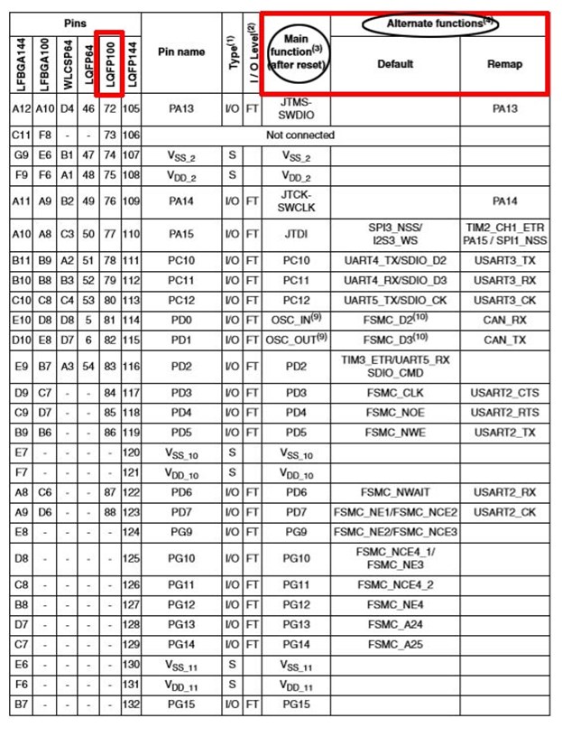
The MCU type used is STM32F103RB, so this is a table assigned with reference to the microcontroller data sheet (link stm32f103xrb data sheet.pdf).
Assign functions to the corresponding MCU pins in the datasheet so that they do not interfere with each other.. In the case of an instructional board, these pins correspond to LQFP64. Each pin has three types of functions: the main function immediately after reset (main), the default function for alternate functions (default), and the remap function (remap).
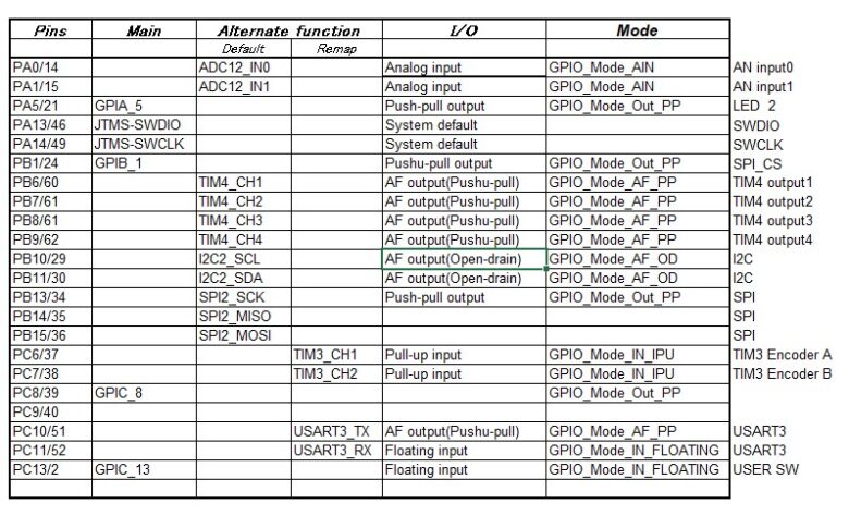
The following is an example of an IO map with IOs assigned to an instructional board.
As you can see from the table, functions are remapped and assigned as needed. Creating a table like this that can be seen at a glance makes it much easier to manage IO when creating programs.
The Modes in the table are those defined in the Standard Peripheral Libraries (SPL), so if HAL is used in the library, this part must be changed accordingly.
MCU has a limited number of pins, so functions must be assigned within this range. In the example of the teaching material board, I want to use multiple TIMs in particular, so I remap the pins to assign functions that do not interfere with each other.
The pins of MCU are GPIOs unless otherwise specified. If you want to specify an alternate function such as TIM, set the pin mode to alternate (AF) when setting GPIO, and specify each alternate function. If remapping is required, it is done at the time of GPIO setting.
The IO allocation map is specifically shown on the actual teaching material board, but it will be of great help when developing other applications as well.