Basic hardware circuits around Microcontroller [Must-see for beginners]
Table of contents
- 1 Electric Circuits and Ohm's Law
- 2 Voltage divider circuit
- 3 Digital Basic Circuit
- 4 Circuit used for General-purpose input
- 5 Input Pull-up/Pull-down Circuit
- 6 Circuit used for General-purpose output
- 7 MOSFETs as switches
- 8 Push-pull output (voltage output), open drain output
- 9 Output configuration circuit by CMOS
- 10 Output interface
- 11 About switches (Momentary and Alternate)
Electric Circuits and Ohm's Law

The electrical circuits used around MCUs are DC circuits, so they are not so difficult to understand if you know Ohm's law. However, it is necessary to familiarize yourself with the circuit because it is somewhat different from the circuits described in textbooks.
The circuits are naturally all connected, but in the notation, the power supply voltage and ground (GND) are shown in an simplified diagram that separates them. From the power supply voltage, the circuit (load) passes through some circuit (load) and returns to the ground (GND) in succession.
The left figure below is a wiring diagram rather than a circuit diagram found in textbooks. In actual circuits, ground (GND) needs to be considered and is shown in the middle of the figure below. In the actual drawing, this is simplified and shown as the right figure below.
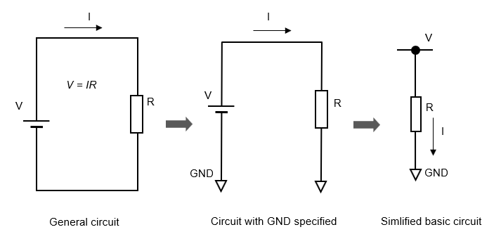
This is where the concept of ground (GND) comes in. In MCU circuits, ground (GND) is the reference potential of the circuit. The unit of electric potential is V, which indicates how high or low the potential is electrically in relation to the reference. The difference in potential between two points is called the potential difference or voltage.
The power supply voltage, for example, is the potential difference of this ground (GND) with respect to the reference potential, so it is easy to understand if the potential of the ground (GND) is defined as the reference value 0V. However, please keep in mind that the ground potential is not an absolute 0V, but a relative 0V as a reference value.
Concepts such as ground and earth are very deep, but in actual circuit design around MCUs, they are very important for practical devices.
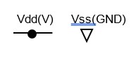
In circuit diagrams around MCUs, power and ground are often shown separately. Since MCUs are digital circuits, electrical signals are either Vdd, the power supply voltage level (common notation in digital circuits), or Vss, the ground level (common notation in digital circuits). In digital logic, a signal level of Vdd is said to be 1 or "H" level (High), while a signal level of Vss is 0 or "L" level (Low).
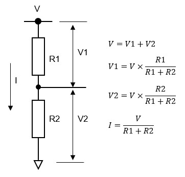
Voltage divider circuit
In a simplified circuit, the voltage divider with resistors will also be easier to understand.
Digital Basic Circuit
Let's look at the operation in the following basic digital circuit.
In the basic circuit 1, a load resistor R is connected to the power supply side (Vdd) and a switch is connected to the ground side (Vss). How does the potential at the midpoint of the circuit change when the switch is turned on or off?
When the switch is OFF, no current flows through the load resistor. Therefore, no voltage is applied to both ends of the resistor and the potential at the midpoint is the same as the supply voltage. In other words, 1 (Vdd). When the switch is turned ON, current flows through the load resistor and the midpoint is equipotential with the ground side of the switch (Vss). In other words, 0 (Vss).
Basic circuit 2 is a circuit in which the load resistor and switch positions are switched in basic circuit 1. Tracing the operation as in Basic Circuit 1, the potential at the midpoint is 0 (Vss) when the switch is OFF, and the potential at the midpoint is 1 (Vdd) when the switch is ON.
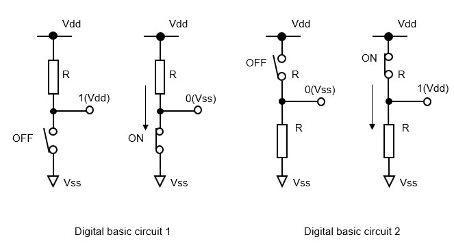
In an electric circuit, a load resistor R is required. In the above figure, if there is no load, a short circuit (short circuit) will occur the moment the switch is turned ON. The value of the load R is explained in "Input Pull-up/Pull-down Circuit" below.
Circuit used for General-purpose input
The input port of the microcontroller has the function of reading the 0 or 1 signal input to the pin.
The 0 or 1 signal is the ground level Vss and supply voltage level Vdd, respectively.
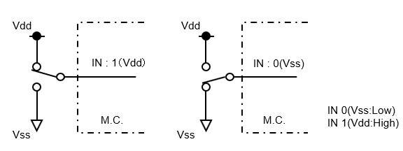
The circuit with the two-way switch below is a simplified representation of a digital input.
Input 1 (Vdd) is on the supply voltage side and input 0 (Vss) is on the ground side.
Input Pull-up/Pull-down Circuit
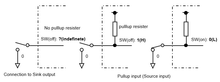
In fact, some of the things connected to the MCU as inputs, such as sensor outputs and switch contacts, do not generate voltage as they are, and cannot give 0 and 1 signals directly to the input ports simply by connecting them like a two-way switch directly connected to the power supply. This way
When a sink output type (see Column 1) is connected as an input, where one of the switch or sensor outputs is ground level Vss, the input port state is 0 when the switch is ON, but the input is indeterminate (floating) because it is not connected anywhere when nothing is done, that is, when the switch is OFF.
A pull-up resistor is used to set the input port state to 1 when the switch is OFF. With a pull-up resistor, the state to the input port is fixed at 1 even when there is no input.
When a source output type (see column 1) is connected as an input, where one of the switch or sensor outputs is at the power supply level Vdd, the input port state is 1 when the switch is ON, but the input is indeterminate (floating) because it is not connected anywhere when nothing is done, that is, when the switch is OFF.
A pull-down resistor is used to set the input port state to 0 when the switch is OFF. With a pull-down resistor, the state to the input port is fixed at 0 even when the input is empty.
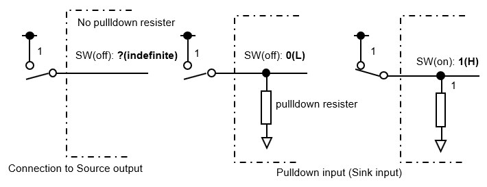
The pull-up and pull-down resistor values range from 300 Ω to 100 kΩ, and although this value should not be determined arbitrarily, many people generally use about 10 kΩ.
A larger value has the advantage of lower power consumption because the current flowing through the load is smaller. However, if the value is too large, the input voltage will drop below Vdd because of the voltage drop across the resistor even at small currents.
MCU input is a circuit composed of C-MOS, which has a high impedance (see Column 2), meaning that current is unlikely to be generated, so this voltage drop does not need to be considered. However, if the value is too large, the change in voltage drop will be greatly amplified by minute changes in current, making it susceptible to noise. The input impedance is like an input resistance and can be checked in the specification sheet of MCU.
In circuits other than MCUs, pull-up and pull-down resistor values are determined by considering the drive current required for the next stage of the circuit. This is because some components will not operate if the drive current is too small. Although the final resistor value should be determined by considering the balance, it is better to refer to the resistors actually used in other circuits.
About Sink and Source
Input side: The source input is the type where the load is connected to a voltage source, and the sink input is the type where the load is connected to ground.
Output side: The source output is connected to the sink input with a power-level output (e.g., PNP transistor), and the sink output is connected to the source input with a ground-level output (e.g., NPN transistor).
Impedance is the resistance (resistance to current flow) in circuits, including AC circuits. The impedance (resistance to current flow) of coils and capacitors changes with frequency. This may sound technical, but phase also changes. As the frequency increases, the impedance of a coil increases, while that of a capacitor decreases. In a DC circuit, it is the resistance itself.
Circuit used for General-purpose output
The output of MCU consists of a semiconductor switching element called a C-MOS. Before explaining the operation of a C-MOS, let us consider the semiconductor switching element.
The basic semiconductor switch is the transistor. Transistors have been used as amplifiers to amplify minute signals into large signals, but in the digital world, including microcomputers, they are used in the role of switches.
A transistor consists of three terminals: base B, collector C, and emitter E. Here, we will use the NPN type transistor shown in the figure below.
When base current IB flows through an appropriate load resistor at base B, collector current IC flows from collector C to emitter E. The collector current IC can be several hundred times larger than the base current IB. The reason transistors are called amplifiers is that they amplify this minute current IB to a large current IC. (However, the collector, which carries a large current, must be connected to an equivalent power supply.)
If the minute base current IB is finely controlled, the collector current IC will be proportional to its magnitude. When the base current IB reaches a certain point, the collector current IC hits its peak and does not increase any further. This is called saturation.
In analog circuit amplifiers, it is important to reach saturation, and the transistor as a switch uses this saturated state with the collector C and emitter E conducting. In other words, two states are used: transistor OFF state with base current IB = 0 and IC = 0, and transistor ON state with base current IB above the threshold ION to turn ON.。
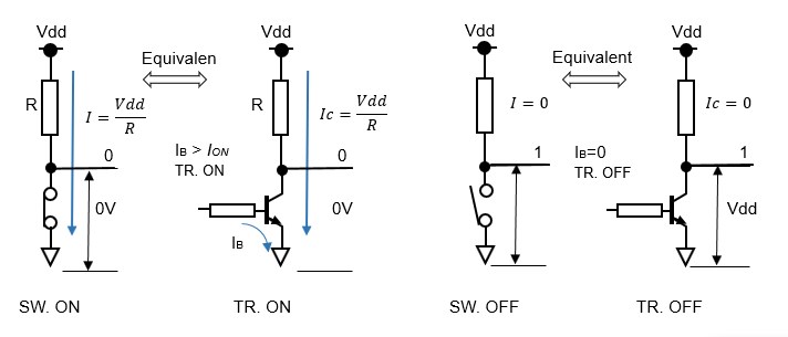
The transistor would be a current-driven switch that is turned on and off by the base current IB.
MOSFETs as switches
So far, I have explained this with transistors, which are the basic semiconductor switches.
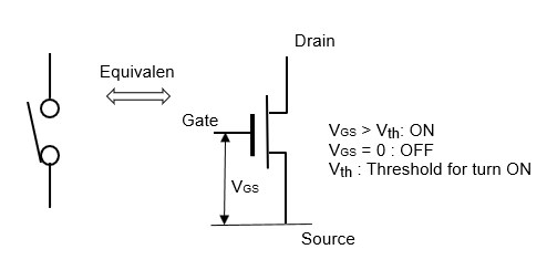
In fact, MOSFETs (field-effect transistors) are used instead of transistors in microcontroller switches.
Understand that a transistor is a current-driven switch that amplifies current, whereas a MOSFET is a voltage-driven switch whose resistance changes when a voltage is applied to its gate.
The gate input impedance of a MOSFET is so high that little current flows even when a drive voltage is applied. In other words, this is a more efficient integrated circuit as a switch inside a MCU because it consumes less power.
Although MOSFETs have an advantage over transistors as switches for MCUs, their disadvantage is that their characteristics are weak against static electricity. The reason MCUs are week against static electricity is that their ICs are composed of MOSFETs.
Despite the differences in characteristics between transistors and MOSFETs, their operation as semiconductor switches is almost the same. The circuits used in MCUs are MOSFETs, so I will use these in my discussion from now on.
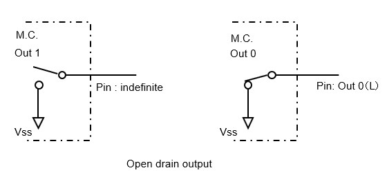
Push-pull output (voltage output), open drain output
MCU general-purpose output ports output 1 (High) or 0 (Low) information.
In what is called a push-pull output type, the output pin outputs a voltage level of either 1 (High) when outputting data 1 or 0 (Low) when outputting data 0.
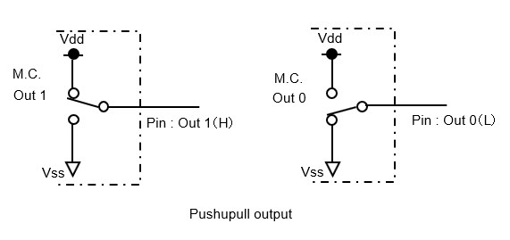
In contrast, in the open-drain output, the output pin is 0 (Low) when the output data is 0, but when the output data is 1, the output pin is a floating type with indeterminate voltage.
These two types of general-purpose outputs are available and should be selected according to the application.
In the case of a transistor, it is called an Open-collector output.
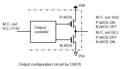
Output configuration circuit by CMOS
Push-pull output circuit
The output circuit of MCU consists of a C-MOS (Complementary MOS) circuit, which is a symmetrical configuration of P-type (P-MOS) and N-type (N-MOS) MOSFETs. When MCU output is 1 (High), the P-MOS turns ON and the symmetrical N-MOS turns OFF. When MCU output is 0 (Low), the P-MOS turns off and the symmetrical N-MOS turns on. In other words, this is a push-pull output circuit.
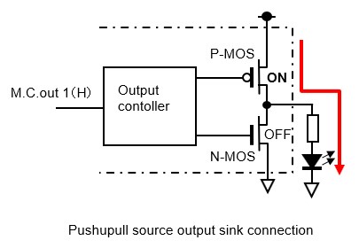
Let's check the operation of a circuit in which an LED is sink-connected as a load to a C-MOS push-pull output circuit.
When MCU output is 1 (High), the P-MOS turns ON and connects to the power supply Vdd. the N-MOS turns OFF and disconnects. As a result, the output pin is set to 1 (High) and current flows through the LED to light it.
When MCU output is 0 (Low), the P-MOS is turned OFF and disconnected from the power supply Vdd. N-MOS is turned on and connected to ground Vss. As a result, the output pin is 0 (Low) and the LED is OFF because both ends are connected to Vss.
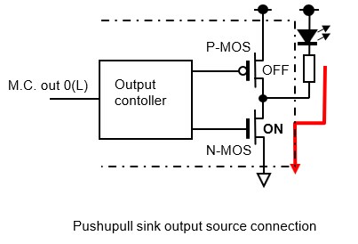
Let's check the operation of a circuit with an LED source-connected as a load to a C-MOS push-pull output circuit.
When MCU output is 0 (Low), N-MOS turns ON and connects to ground Vss. P-MOS turns OFF and disconnects. As a result, the output pin is 0 (Low) and current flows through the LED to light it.
When MCU output is 1 (High), N-MOS is turned OFF and disconnected from ground Vss. P-MOS is turned ONand connected to power supply Vdd. As a result, the output pin is set to 1 (High) and the LED turns OFF because both ends are connected to Vdd and no current flows.
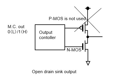
Open-drain output circuit
If an open-drain is selected for the output, it is safe to assume that the P-MOS is disabled and not used.
Therefore, when the microcontroller output is 1 (High), the N-MOS is also off and the output pin is not connected to anywhere. When the MCU output is 0 (Low), the N-MOS turns on and connects to ground Vss, so the output pin becomes 0 (Low).
Output interface
Transistor-based interface
The output port of MCU is a circuit consisting of a C-MOS. The maximum allowable current for the output pins of this C-MOS is determined; in the case of the STM32 MCU, the maximum allowable current is 8 mA per port.
If the current flowing through the load is small, such as an LED, it can be connected directly to the output pin, but not all loads that you want to drive with the output (loads you want to connect to the output) are resistive loads that function with a small drive current, such as LEDs.
Examples include inductive loads such as relays and motors, and loads with large drive currents such as heaters. Even in the case of LEDs with a small load capacity per LED, the allowable current of MCU will be exceeded if the number of LEDs is large.
In such cases, interface circuits are provided between MCU and the load to drive the LEDs.
Let's look at a circuit that uses a transistor as an interface to drive an LED. When the microcontroller output port is 1 (High), the base current flows to the transistor and it turns ON and conducts. As a result, current flows to the LED and it turns ON.
Since the transistor has a current amplification function, the collector current that can flow to the load LED can be as large as the power supply capacity allows in relation to the base current. In other words, since the base current is small, the load current can flow without worrying about the allowable current of MUC.
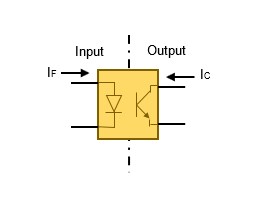
Interfaces using optocouplers
Let's look at a circuit that drives a load via an interface called a optocoupler to a MCU output.
An optocoupler is an element in which the input and output sides are electrically isolated. By keeping the power supply on the input side separate from the power supply on the output side, noise generated on the load side can be isolated to prevent malfunctioning of the microcontroller.
The optocoupler is a switch that drives a light-emitting diode on the input side and turns on/off a phototransistor on the output side. It can drive a load within the allowable range of the output side transistor.
In the output interface with optocoupler, the MCU output drives the optocoupler light-emitting diode to turn on the output transistor. The drive current IF is adjusted by the resistor R.
In the input interface with optocoupler, the output transistor is turned on by driving the photocoupler light-emitting diode with an external switch or other means. The drive current IF is adjusted by a resistor R.
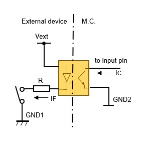
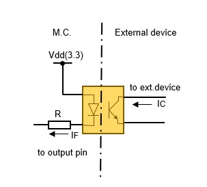
It is similar to the case where a transistor is used as an interface, but the optocoupler differs in that the input and output are electrically isolated from each other. Depending on the specifications of the optocoupler, the current amplification factor may not be as large as that of a transistor, so the load current should be carefully checked in the specification sheet when selecting the optocoupler..
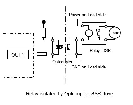
In industrial equipment, input/output devices such as sensors and MCUs are often used with separate power supplies. It is an ironclad rule to separate the power supplies for expensive sensors and other devices from that for MCU, taking noise and other effects into consideration.
A PLC (Programmable Logic Controller), a type of embedded device specialized for machine control, has output types such as transistors and relays, but is separated from the internal MCU by a optocoupler, making it a robust system against noise.
The figure shows a circuit in which a relay is driven via an optocoupler. The relay opens and closes its contact points according to the voltage and current signals given to the input coil. Relays are useful in electric circuits where switches are automatically switched by a program.
The coil at the relay input cannot be directly driven by MCU output because it is an inductive load and generates a back EMF. Therefore, the relay is driven via an optocoupler. The figure is a simplified illustration to explain the operation. In reality, a protection diode or other device is required to protect the relay from the back EMF generated by the coil.
The relay is called a contact, which mechanically turns the contact on the load side on and off. Therefore, the contacts wear out and need to be replaced according to the number of open/closed cycles. In contrast to these mechanically configured relays, SSRs (Solid State Relays) are contactless relays that are configured with semiconductors. SSRs are often used to control heaters, etc. Since they do not have mechanical contacts, they have features such as high operating speed and no contact wear.
Details of designing with photocouplers are explained in "Embedded Hardware design [with Specific circuits]".
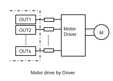
Interface using dedicated ICs
To control DC motors, stepping motors, etc., a circuit is composed of a combination of semiconductor switches such as transistors to drive them. It is convenient to use a dedicated driver IC with all functions built into a single package, which requires fewer components and is advantageous in terms of performance and cost.
The input side of the driver IC only needs to be provided according to the specifications of each driver. For actual development, as soon as the target motor specifications are determined, commercially available driver ICs are selected based on performance, price, and availability (ease of acquisition).
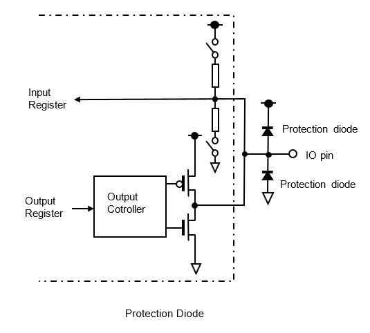
Protection Diode
The IO port of MCU has a built-in protection diode, which is called a clamp circuit. It protects the circuit from signal overvoltage (e.g. surge voltage) and electrostatic discharge (ESD).
The diode configuration shown in the figure limits the signal voltage at the IO port to within the range even if it exceeds the range from Vss (GND) to Vdd (supply voltage).
About switches (Momentary and Alternate)
There are two types of operating switch actions: Momentary and Alternate.
Momentary action :
The Momentary is ON for as long as the switch button is held down, and returns to OFF when the button is released. Momentary" means "temporary" or "instantaneous.
Alternate action :
The Alternate turns ON when the button is pressed once and remains ON even when the button is released. Pressing the button again turns it OFF. It is called a self-holding type switch. Alternate" means "alternately" or "alternating.
If the switches connected to the input pins of MCU are of the momentary operation type, they can be combined with counters and timers to provide various functions.